I have a few opinions about the critical need for more focus on better materials and better fabrication techniques in the superconducting qubit community to help solve long-running issues with qubit coherence, qubit targeting, etc. So it was with some delight that I found this (pretty dope) paper published to the arXiv by the IBMQ team.
Laser-annealing Josephson junctions for yielding scaled-up superconducting quantum processors.
Abstract
As superconducting quantum circuits scale to larger sizes, the problem of frequency crowding proves a formidable task. Here we present a solution for this problem in fixed-frequency qubit architectures. By systematically adjusting qubit frequencies post-fabrication, we show a nearly ten-fold improvement in the precision of setting qubit frequencies. To assess scalability, we identify the types of ‘frequency collisions’ that will impair a transmon qubit and cross-resonance gate architecture. Using statistical modeling, we compute the probability of evading all such conditions, as a function of qubit frequency precision. We find that without post-fabrication tuning, the probability of finding a workable lattice quickly approaches 0. However with the demonstrated precisions it is possible to find collision-free lattices with favorable yield. These techniques and models are currently employed in available quantum systems and will be indispensable as systems continue to scale to larger sizes.
The problem is this: the current IBM junction fabrication process yields qubits with a very large frequency distribution around the target frequency. The frequency of a transmon, the workhorse of the superconducting quantum computing world, is given approximately by \(f_{01} \sim \sqrt{8E_jE_c} - E_c\), where the Josephson energy, \(E_j\) depends linearly on the Josephson junction critical current, \(I_c\). What IBM (and many others) care about is the goodness of the frequency targeting of their qubits. What determines good frequency targeting is actually Josephson junction critical current targeting during the fabrication process. IBM uses fixed-frequency qubits, so getting this right during fabrication is doubly important. Once the qubits are in a refrigerator, there can be no adjustments!
Why does frequency targeting matter? The strength of qubit-qubit interactions, an important part of quantum gate operations, are determined in part by the difference in frequency between two interacting qubits. IBM performs what they term ‘cross-resonance gates’, where one qubit is driven at the frequency of its interacting partner. This approach relies on a precisely calibrated frequency difference between the qubits, so deviations from this precise calibration can be disastrous, especially when the frequencies of the two qubits ‘collide’.
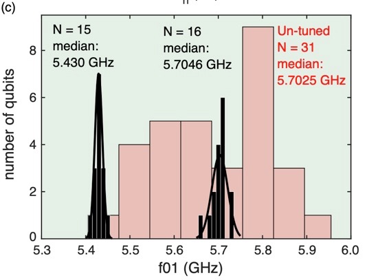
We can see from Fig 1b and 1c (see below) in the paper that the junction frequency targeting of the native, non-altered fabrication process is very bad. The transmons are fabricated with a median frequency of \(5.70 \pm 0.13\) GHz. What the figures show is that the highest and lowest frequency transmons come in nearly \(300\) MHz above/below the median! A distribution this wide makes it impossibly difficult to target two or more separate frequency bands without incurring frequency collisions.
It’s been known for a little while that thermally annealing the metal-oxide insulator in the Josephson junction can increase the resistance, \(R_n\), of the tunnel barrier created by the oxide layer. This has the practical effect of changing the Junction critical current, since \(I_c = \frac{\pi\Delta}{2eR_n}\). Throwing a whole chip in the oven won’t solve your frequency crowding problem, since the anneal is applied globally. What if you could anneal individual junctions, though? What if you could do that, and tune exactly how much you change the \(R_n\) of the junctions? Well you can, if you happen to have a sufficiently powerful laser and the right optical setup! Shockingly, this procedure was demonstrated 12 years ago by an Italian group and published as a proceeding of the EUCAS conference. It has exactly one citation: the IBM paper.
The IBM team built an apparatus that can step through an entire chip, shining a laser whose power and illumination duration is precisely calibrated to give the required increase in \(R_n\). In this way, they take their original 31 qubit distribution with enormous spread and turn it into two, very tight clusters of 15 and 16 qubits. I have included the relevant figure below.

Histogram of transmon frequencies pre- and post- laser annealing. From Laser-annealing Josephson junctions for yielding scaled-up superconducting quantum processors by JB Hertzberg et al., https://arxiv.org/pdf/2009.00781.pdf
They claim to have a ‘combined’ frequency spread of \(\sigma_f\) = 14 MHz, but based on this figure that seems… optimistic. It’s hard to tell, but I think the transmon bunch centered around 5.7 GHz seems to have a full width of the fit that is around 50 MHz. Still, reducing frequency spread among qubits by nearly an order of magnitude is a remarkable achievement.
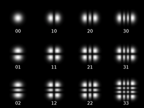
It’s a shame that aside from basically saying “we used a laser to make the substrate hot” no details are given about the procedure. Figure 2 has a block diagram of the setup, fine. Sentences like “The beam is shaped as necessary to avoid direct illumination of the junction, and beam size is condensed 4x using a dual-objective setup [40]” are very much not helpful when the reference leads to the US patent for this technique. To save you the trouble, I have read through it to find the details of beam size and shape. It turns out that the team uses an axicon lens to transform a Gaussian beam into an annulus with a dark center. The outer radius of the annulus comes in at about 10 \(\mu m\), so a Josephson junction could probably comfortably fit inside the dark zone. This is how they avoid hitting the junction itself with laser light. Instead the laser should end up more or less evenly heating the substrate around the junction. I’m curious to know why they chose an annulus (the 01 Laguerre-Gauss mode) which will intersect the aluminum finger that forms part of the Josephson junction, rather than using the 10 or 01 Hermite-Gauss mode which would put two blobs of light on either side of the junction (see figure below).

Fig2. The Hermite-Gauss beam modes
It’s unclear to me why the interesting optical details were hidden at the end of a very lengthy, nearly inscrutable patent instead of clearly laid out in a paper titled “Laser-annealing Josephson junctions for yielding scaled-up superconducting quantum processors”. Or why no concrete discussion of laser powers and energy flux exists. Another mysterious omission is the lack of any commentary on qubit coherence after the annealing process. We know that they use Ramsey fringes to determine the qubit frequencies, so the coherence can’t be zero, but is it impacted by the process at all?
The rest of the paper is devoted to categorizing types of frequency collision and how they will impact the various available quantum processor architectures on the table. For a standard square lattice of qubits, even the improved laser-annealing process has poor frequency-collision free yield for 49 qubits (\(<0.1\%\)) and abysmal yield for a 97 qubit lattice (\(\ll0.1\%\)). Modified lattices, shown in the supplementary text, have better yield. The lattices with largest code distances (\(> 100\) qubits) have yields in the \(6-8\%\) range which suggests that it’ll take something like 10-20 chips to find one pristine candidate.
According to the IBM Quantum Roadmap, we should expect to see the \(127\) qubit heavy hexagon lattice debuted by 2021. By 2023, we should expect to see a \(1,000\) qubit chip. Note that, for the heavy hexagon lattice, taking the code from \(65\) to \(127\) qubits caused a \(4\)x reduction in expected collision free chip yield. The current state of laser-anneal frequency tuning simply cannot produce a collisionless \(1,000\) qubit chip. Indeed, figure 4 in the paper shows that a \(1,000\) qubit heavy hex processor will require a \(\sigma_f < 10\) MHz to have yields better than \(1\%\). That’s an additional \(30\%\) reduction in frequency spread. The authors themselves estimate that they’ll need a 2x reduction in frequency spread to reliable achieve 1,000 qubit processors. They also point out that the precision of current laser-anneal technique is basically limited by the precision with which they can estimate the frequency of a transmon from its junction \(R_n\). It’s worth noting that they can set the value of junction \(R_n\) with \(0.3\%\) precision, which translates to \(0.15\%\) precision in the qubit frequency. If that is the only source of error in the qubit frequencies (it’s not), then for a qubit with frequency tuned to be \(5.7\) GHz, we would expect the frequency spread to be \(8\) MHz. That happens to be the level of imprecision required to make the \(1,000\) qubit processor at all feasible. The take-away for me is that, in order to move beyond \(1,000\) qubits, IBM must demonstrate not only an improvement in qubit frequency prediction from \(R_n\), but also an improvement in the precision to which the \(R_n\) can be tuned with the laser anneal.
Overall, this is a cool paper describing the success of a precision qubit frequency tuning technique that doesn’t require any extra fabrication steps, and doesn’t require cryogenic temperatures to implement. The laser-anneal should enable IBM to produce chips with architectures up to \(100\) qubits, but will need to improve the frequency precision by a factor of \(2\) to get to \(1,000\) qubits, which is the current fundamental limit of the technology. Not sure how they plan to get to \(1,000,000\) qubits, but I guess we’ll find out in a few years.